Home / Semiconductors /
What is an SCR?
The SCR (Silicon Controlled Rectifier) is a 4-layer semiconductor device that works as an almost ideal switch. Its symbol and structure are shown in the first image. A = anode, G = gate, and K = cathode.
SCR works as a controlled rectifier diode that allows the flow of the electric current only in one direction.
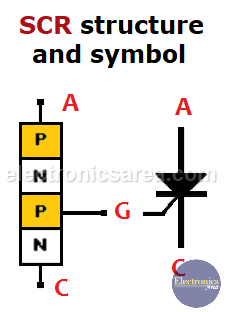
A = anode, G = gate and C = K = cathode
Basic Operation
If no voltage is applied to the gate of the SCR, there is no conduction of current from the anode to the cathode, so it works like an open circuit. On the contrary, if there is a voltage applied to the gate of the SCR, it begins conducting, and there is a flow of current from the anode to the cathode, so it works like a short circuit.
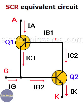
To better understand its basic operation, an equivalent circuit of the SCR is shown in the image below.
- When an IG current is applied to the G terminal (base of Q2 and collector of Q1), two currents are produced: IC2 = IB1.
- IB1 is the base current of transistor Q1 and causes a collector current of Q1 (IC1) to flow.
- IC1 in turn feeds the base of transistor Q2 (IB2), which causes more current in IC2, which is the same current IB1 at the base of Q1, and …
- This regenerative process is repeated until transistors Q1 and Q2 become saturated, causing the SCR to conduct and operate like a short circuit.
Parameters are:
- VRDM: Maximum reverse voltage (VG = 0)
- VFOM: Maximum direct voltage (VG = 0)
- IF: Maximum allowed direct current
- PG: Maximum dissipation of power between gate and cathode.
- TGV-IGT: Maximum voltage-current required in the gate (G) to trigger the SCR
- IH: Minimum anode current required to keep the thyristor in its ON state
- dv/dt: Maximum voltage variation without triggering.
- di/dt: Maximum accepted current variation before destroying the thyristor.
Note: dv/dt and di/dt: See parameters of SCR in DC.
Characteristic curve of the SCR
The picture below shows the relation between the switching voltage and the gate current.
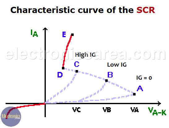
- When it is reverse-biased, it operates like a common diode (see the leakage current feature).
- When it is in the direct bias region, it also operates like a common diode, but it has already been activated (on). See points D and E (high conduction).
For high gate current (IG) values (see point C), the anode-cathode voltage is lower (VC).
If the IG decreases, the anode-cathode voltage increases. (See points B and A and anode-cathode voltages VA and VB). In conclusion, if we reduce the gate IG current, the anode-cathode voltage will tend to increase before the SCR is ON.
Below are two SCRs of different power. The more powerful one is on the left.
100 Amps/800 Volt: left side—13 amps/800 Volt: right side.
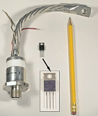
Thuringius [CC BY-SA 3.0], via Wikimedia Commons
You may also like:
- The TRIAC (Triode for Alternating Current)
- The DIAC (Diode for Alternating Current)
- The SBS (Silicon Bidirectional Witch)
Applications of Silicon-Controlled Rectifier
- As an AC voltage stabilizer
- In battery chargers
- As switch
- For power control
- In inverters (to switch from DC voltage to AC voltage)
- etc.
Some circuits that use an SCR:
- Fire alarm circuit using thermostats and SCR
- 12V auto-turn-off battery charger circuit
- Thermistor-controlled fan Circuit – AC fan


