Home / Semiconductors /
What are MOSFET transistors?
MOSFET transistors, or Metal-Oxide-Semiconductor (MOS) transistors, are field-effect devices that use the electric field to create a conduction channel. MOSFET transistors are more important than JFETs because almost all integrated circuits (ICs) are built with the MOS technology.
There are two kinds of MOSFET transistors:
- N-channel MOSFET transistor, or NMOS
- P-channel MOSFET transistor, or PMOS
At the same time, they can be enhancement transistors or depletion transistors. In the present days the last ones are not used. In these tutorials, we will describe only the enhanced MOS transistor.
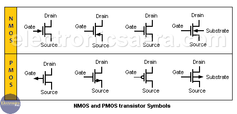
NMOS and PMOS Symbols
The following image shows the different symbols used to describe the MOS transistor.
MOSFET transistors (NMOS) physical structure
The next image shows the N-channel MOSFET transistor’s physical structure with its four terminals: gate, drain, source, and substrate. Normally, the source and the substrate are connected together.
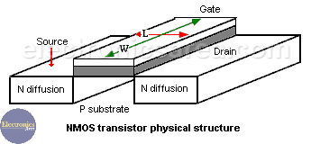
The gate with W and L dimensions is separated from the substrate by a dielectric (SiO₂), creating a similar structure to the capacitor plates.
If a positive voltage is applied to the gate, negative charges are induced (inversion layer) on the substrate surface, and they create a conduction path between the drain and source terminals.
The minimum voltage needed to create the inversion layer is called the threshold voltage (VT). This is a characteristic feature of the transistor. If VGS < VT, the drain-source current is zero. Typical values for this voltage are between 0.5 and 3 volts.
NMOSFET operating regions
JFET and MOSFET transistors have a very different physical structure, but their analytical equations are very similar. In the MOSFET transistors, the same regions of operation are defined: cutoff, linear, saturation, and breakdown.
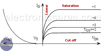
The image shows the curves of electrical characteristics of an NMOS transistor with the different regions of operation. These regions of operation are briefly described below.
NMOS FET Cutoff region
We can verify that VGS < VT and the current ID is zero.
NMOS FET Linear region
The transistor behaves as a nonlinear resistive element, controlled by voltage. Check the following equations:
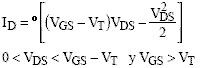
where:

is a characteristic parameter of the MOS transistor, which depends on the k constant and the size of the transistor gate (width W and length L).
NMOS FET Saturation region
The NMOSFET transistor behaves as a voltage-controlled current source (VGS). Check the following equations:
![]()
where ß = K (W/L)
In this region, the quadratic relationship between VGS and ID is shown in the left part of the picture. Similarly to the JFET transistors, it can be used to identify, by graphical methods, the bias point of the transistors. This method is rarely used.
NMOS FET Breakdown region
A MOS transistor can be affected by the avalanche phenomenon in the drain and source terminals. The MOS transistor can also be affected by breaks in the thin oxide layer of the gate that may destroy the device.
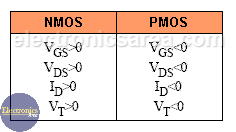
Finally, note that the table above shows the differences in sign and direction of the currents and voltages between NMOS and PMOS transistors.
MOSFET transistors are field-effect devices that use the electric field to create a conduction channel. There are 2 kinds of MOS transistors: NMOS and PMOS


