JFET Saturation and Breakdown regions
The JFET Saturation region
In this region the JFET has some linear features that are used in amplification. These features are similar to those of a BJT in the linear region. The JFET behaves as a voltage controlled (VGS) current source which ID is virtually independent of the voltage VDS.
The equation that relates the current ID with the voltage VGS is known as the Schockley equation that is given by:
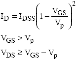
where Vp is the pinch-off voltage and IDSS is the saturation current.
This current (IDSS) is defined as the value of the current ID when VGS = 0, and this feature is often used to obtain a constant value current source (IDSS). This equation at the ID and VGS plane represent a parable displaced in Vp.
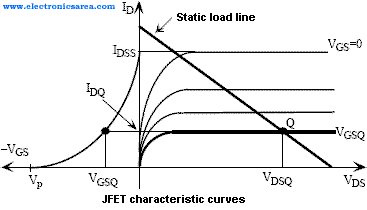
This relationship with the characteristics of the JFET of Figure 1.11 (see this link), allow us graphically how to find the Q point of the JFET transistor in the saturation region.
The following figure shows the graphic representation of the Q point and the relationship between both curves which help to find the bias point of the JFET transistor using graphics.
The JFET Breakdown region
A high voltage at the terminals of JFET transistor can lead to a breakdown through the gate junction. The manufacturer specifications show the breakdown voltage between the drain and the source terminals when the gate and the source terminals are joined. This voltage is knowned as BVDSS and its value is between 20 and 50 volts. These bias voltages do not have to be greater than these values in order to avoid the deterioration of the device.
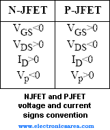
Differences between the NJFET and the PJFET
The equations showned above for the JFET are valid for the PJFET taking into account the signs convention of the next table


 - Thyristor")